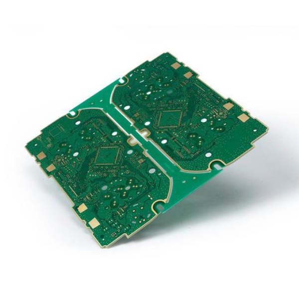
A Multilayer PCB is a circuit board consisting of three or more conductive copper layers laminated together with insulating dielectric material. Unlike single or double-layer boards, these complex structures allow for highly dense routing and superior electrical performance. The layers are bonded under heat and pressure, with vias (PTH) connecting the circuits across different levels to maximize functionality within a compact form factor.
Key Features
Layer Count: Typically ranges from 4 to 20+ layers (customizable up to 40+ layers).
Construction: Alternating layers of Copper and Prepreg/Core materials.
Via Technology: Supports Through-Hole, Blind, Buried, and Micro Vias for high-density interconnection.
Thickness: Standard 0.8mm – 3.2mm (customizable).
Surface Finish: Options include HASL, ENIG, OSP, Immersion Silver/Tin.
Material Options: Standard FR4, High-Tg FR4, Rogers, Polyimide, or Hybrid laminates.
Advantages
High Density & Compact Size
- Consolidates complex circuitry into a single board, reducing overall footprint and weight.
Superior Signal Integrity
- Controlled impedance and reduced cross-talk make it ideal for high-frequency transmissions.
Enhanced Durability
- Utilizes high-Tg materials and thicker copper to withstand thermal and mechanical stress.
Improved Power Management
- Dedicated power and ground planes minimize voltage drops and electromagnetic interference (EMI).
Greater Flexibility in Design
- Blind/Buried vias allow for intricate routing that is impossible on 2-layer boards.
Reliability
- Fewer connectors and wiring points compared to stacking multiple double-sided boards.
Applications
Telecommunications: 5G base stations, routers, and high-frequency servers.
Medical Devices: MRI machines, CT scanners, patient monitoring systems.
Industrial Control: Motor drives, power inverters, and robotic controllers.
Consumer Electronics: Smartphones, laptops, and wearable technology.
Automotive: ADAS (Advanced Driver Assistance Systems), engine control units, and infotainment.
Aerospace & Military: Radar systems, navigation equipment, and satellite communications.
Why Choose Our Multilayer PCBs?
We utilize precision layer alignment technology and strict impedance control to ensure your high-speed designs perform flawlessly. Whether you need quick-turn prototyping or high-volume production, we deliver reliability layer by layer.